GPIO stands for General Purpose Input Output and refers to the fact that the pins can support both output and input functionalities. Looking physically at any microcontroller you can readily see rows of pins that allow the microcontroller to control and communicate with outside devices. Lets take a look at the pinout diagram of the G2553 device as provided by TI on page 3 of the MSP430G2553 datasheet:
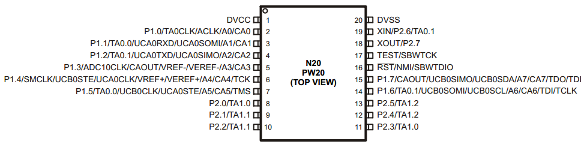
Looking at the pins in the diagram we notice that each pin has a long name, with several designations separated by a slash. Because microcontrollers have a limited number of pins and at the same time a large number of peripherals, the manufacturer has to multiplex the pins among the internal modules. This means that each pin has a number of functions that it can perform, but only one of them at a time. Most pins of the MSP430 operate as GPIO pins, with a possibility of functioning as a specialized pin in the right configuration. As GPIO pins, each pin is independently controlled and can be made an input and an output, high or low.
You might not realize it, but you have just stumbled upon one of the first thing every embedded designer must do. Because of the limited number of I/O pins and application requirements, you must carefully consider the use of each pin of the design. Pins are not born equal, and in some instances you will save yourself a lot of headache if you consider carefully what you need and what is available. You might even end up changing the microcontroller if the one you currently use doesn’t provide the right mix of GPIO and peripheral pins.
Pins capable of GPIO functionality and control are indicated with the naming PX.Y, where X represents the port number to which the pin belongs and Y represents Pins belonging to port one are denoted by P1.Y, while pins forming Port 2 are named P2.Y where Y is a specific pin number. Notice that some pins are GPIO only, with no specialized function. The bit controlling the pin. The number of Ports and pins is device specific and can be obtained in the device datasheet. The MSP430F2553 has a total of 2 ports, Port 1 and Port 2.
Each port is assigned several 8-bit registers that control the function of the pins and provides information on their current status. The following is a list of registers always available for ports:
Note that each register bit controls only one pin in the port. For example, PxSEL looks as follows:
| SEL P1.7 | SEL P1.6 | SEL P1.5 | SEL P1.4 | SEL P1.3 | SEL P1.2 | SEL P1.1 | SEL P1.0 |
The second number in the port number (Y in PX.Y) tells you which bit controls it. P1.1 is controlled bit 1 in several registers including P1SEL, P1DIR, P1OUT and P1IN working all together to define the functionality of the pin.
Placing a pin in peripheral mode does not set the direction of the pin, which might be required depending on the peripheral. Make sure to consult the peripheral documentation in the Datasheet as to whether setting the direction is required and what is the proper direction.
Saving board space and reducing the number of components is the goal of every engineer. In many cases, GPIO lines need a pull-up or pull-down and integrating it in the MSP430 enables easy configuration and space saving. Some MSP430 support enabling a pull-up or pull-down resistors via software on certain ports. Note that this can only be enabled when the GPIO is in input mode. In order to control this, a few special registers are used:
PxREN only controls whether the functionality is enabled. PxOUT in this mode is the one that controls whether the resistor is pull-up or pull-down. A word of caution is in place. The pull-up and pull-down capability of the MSP430 is limited, with a resistance of about 20k to 50k ohm as shown in the datasheet. Using internal pull-ups in some cases such as I2C is not advisable, but it works well for switches and other cases.
Some GPIOs in the MSP430 have the capability to generate an interrupt and inform the CPU when a transition has occurred. The MSP430 allows flexibility in configuring which GPIO will generate the interrupt, and on what edge (rising or falling). The registers controlling these options are as follows:
PxIES might be a little confusing. One easy way to remember the option is to think of the bit as the initial state. For example, if the bit is 0, the initial state is at 0, and the pin will generate an interrupt going from 0 to 1, a rising edge.
MSP430 devices typically have interrupt capability on Ports 1 and 2. Other ports may not have any capability for interrupts. You must therefore be careful when designing the MSP430 on a board to ensure that the pins are properly allocated so you have interrupt capability.
In the discussion above we always talked about ‘1’ and ‘0’. The reality is that a microcontroller generates a finite voltage representing ‘1’ and ‘0’. Except for a few MSP430 with dual voltage rail capability, the HIGH (1) generated by the GPIO will be close to VCC. This assumes that the load on the GPIO is within reason. The MSP430 like most devices has a limit on the amount of current that can be drawn from the pins, both individually and as a whole. The datasheet of the MSP430 specifies that with 6mA of current draw at a pin the following should hold:
The ramifications are significant. Running the MSP430 at 3.3V will make it difficult to interface to a 1.8V part because the high voltage will likely violate the specifications of the other device. You could run the MSP430 at 1.8V, but there are other considerations such as the frequency dependency of the CPU on voltage. The main point is that you should consider the issues of GPIO loading and voltage in your design because they might be significant.
The MSP430 also requires that applied voltages to pins in input mode be within specification. The MSP430 uses a Schmitt-Trigger at the input of each pin to determine whether the voltage represents a logic High(1) or Low(0). The datasheet specifies what to expect as far as logic thresholds. In general, voltage on the pins should never exceed VCC that is operating the MSP430, and never 3.6V. Although it is possible to operate pins at VCC+0.3V, this triggers the ESD diode structure and may damage the part.
Upon powerup of the MSP430, before any code is executed, the registers controlling the MSP430 are cleared to defaults. This includes PxSEL set to 0, along with PxDIR, meaning that pins are generally configured as inputs with high impedance. In this mode, the pins draw almost no current and thus avoid disturbing the circuit. Although example code sometimes avoid explicitly setting all the configuration registers, we suggest that you be always explicit and never rely on any defaults. One reason is that a custom bootloader may be used that takes control of the GPIO for some purpose and cause problems for the application which fails to initialize all the registers.
We can’t discuss GPIO without showing how to control it. The following examples show how to configure the GPIO as well as use the pin muxing:
Configuring P1.0 as a GPIO Output set to High(1)
#include <msp430.h>
void main()
{
    WDTCTL = WDTPW + WDTHOLD; // Stop watchdog timer
    P1SEL &= (~BIT0); // Set P1.0 SEL for GPIO
    P1DIR |= BIT0; // Set P1.0 as Output
    P1OUT |= BIT0; // Set P1.0 HIGH
}
Configuring P1.0 TA0CLK
#include <msp430.h>
void main()
{
    WDTCTL = WDTPW + WDTHOLD; // Stop watchdog timer
    P1SEL |= (BIT0); // Set P1.0 SEL as TA0CLK
}
Configuring P2.1 for Interrupts
#include <msp430.h>
void main()
{
    WDTCTL = WDTPW + WDTHOLD; // Stop watchdog timer
    P2SEL &= (~BIT1); // Set P2.1 SEL as GPIO
    P2DIR &= (~BIT1); // Set P2.1 SEL as Input
    P2IES |= (BIT1); // Falling Edge 1 -> 0
    P2IFG &= (~BIT1); // Clear interrupt flag for P2.1
    while(1)
    {
        if(P2IFG & BIT1)
        {
        // Do Something
        }
    }
}
The code above shows how it is possible to poll the Interrupt Flag register to check whether an interrupt has occurred, as opposed to having an interrupt routine called. Polling should be generally avoided because of the performance penalty of having the CPU constantly check for the state.
#include <msp430.h>
void main()
{
    WDTCTL = WDTPW + WDTHOLD; // Stop watchdog timer
    P2SEL &= (~BIT1); // Set P2.1 SEL as GPIO
    P2DIR &= (~BIT1); // Set P2.1 SEL as Input
    P2IES |= (BIT1); // Falling Edge 1 -> 0
    P2IFG &= (~BIT1); // Clear interrupt flag for P2.1
    P2IE |= (BIT1); // Enable interrupt for P2.1
    __enable_interrupt(); // Enable Global Interrupts
    while(1)
    {
        if(flag == 1)
        {
            // Do Something
            flag = 0;
        }
    }

}

// Port 1 interrupt service routine
#pragma vector=PORT2_VECTOR
__interrupt void Port_2(void)
{
    flag = 1;
    P1IFG &= (~BIT1); // P2.1 IFG clear
}
The application above makes complete use of interrupts. P2.1 is configured as an input pin with a falling edge interrupt. General interrupts are enabled so that the pin will make the CPU call the Interrupt Service routine. This routine sets a flag that causes some processing to be performed in the main loop.
One of the most common uses for GPIOs is to connect switches, especially momentary buttons for user interfaces. Switches can be connected easily, but require some consideration to use properly. The switch is typically connected between a pin and ground, so that pressing on the switch will cause a falling edge. For this to happen, the pin must be biased at VCC. Typically this means using a pull-up, either internal or external. For external switches, a value of 100k is typical. When the switch is open, the voltage at the pin is basically VCC given the small amount of current flowing results in virtually no voltage drop across the pull-up resistor. When the switch is closed, the pin is connected to ground and the pull-up resistor conducts as well. This current is wasted, which is why large values of pull-up resistors are used.
Up to now we have assumed that the switch is a perfect device with a well defined ON and OFF behavior. In reality, most switches are mechanical and are prone to bouncing. The contacts that are being connected together will take some time to settle. During this time, the electrical circuit will connect and disconnect, causing transients to appear at the pin. These transients are often in microseconds, which means that a microcontroller may see hundreds of transitions for just one press of the button. The first solution to this issue is to use a capacitor placed parallel to the switch to debounce it. When the switch is normally open, the capacitor is charged to VCC. When the user presses the switch, the capacitor begins discharging to ground, but does not do so immediately. During this time, the voltage drops off exponentially and only a single transient is seen by the pin. The speed of the transition depends on the RC constant of the pull-up and capacitor, but values of 10nF to 100nF and 100k typically work well.
Along with a hardware solution, it is possible to use a software timer to perform a software debounce. On the first interrupt you can trigger a timer and disable the GPIO interrupt. After a set amount of time, usually 20ms to 50ms, the timer triggers and its ISR checks whether the switch is still being held (the pin will show low on PxIN). If so, then a button press is handled. Experiments have shown that different buttons behave differently, although 20ms to 50ms is typically the time required for them to completely settle down.
We recommend that you test the buttons in your hardware to see the behaviour of the bouncing. This can be done easily with an oscilloscope connected to the pin.
Lets look at how the MSP430 launchpad designs the switch:
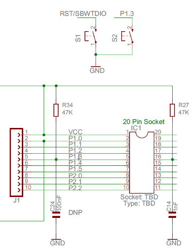
S2 is the switch of interest and it is connected to P1.3. P1.3 has both a 100nF capacitor and 47k ohm pull-up resistor, as was our recommendation above. This results in clean signals at the pin.
Another easy use of GPIOs is for indication using LEDs. An LED can be connected directly to the MSP430 pin. One easy way is to connect the LED as follows:
When the pin is low, the voltage across the LED is almost zero, so it remains off. But, when the pin is high, the voltage causes the LED to turn on. Note that a series resistor is used to reduce the voltage given that most LEDs require around 2V (consult the datasheet for your LED). Values of 220 ohm to 1k ohm are typical. A microcontroller is typically better at sinking current than sourcing it. LEDs can be connected between VCC and the MSP430: The polarities are then reversed. When the MSP430 pin is high, the LED is off because the potential difference between the LED terminals is very small. When the MSP430 pin is set to ‘0’ (Ground), the potential difference is large and the LED turns on.
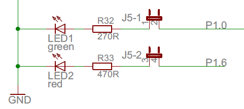
You can see the Launchpad board has two LEDs at P1.0 and P1.6. Each LED has a series resistor with a different value to make the output luminosity more uniform when they are lit.
Enter your email address to subscribe to this blog and receive notifications of new posts by email.