SPI is one of the most common interfaces in Embedded Systems and it is one of the most utilized in the MSP430. Although it requires more pins than UART, its external clock often enables very fast transfers that are more reliable because both ends are synchronized. The MSP430 supports SPI in various modules.
A SPI connection between a Master and a Slave device is shown below:
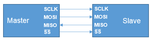
SPI uses the concept of a master device and multiple slave devices. Let’s look at some of the signals:
SPI is a full duplex protocol in which the slave and the master exchange data at each transition of the clock by setting MOSI and MISO to a bit value. Note that MOSI and MISO are descriptive name for the connection. Often times they are called SIMO and SOMI or Slave Output (SO) and Slave Input (SI). It’s very important to avoid mixing the two signals by crossing them. MOSI should connect to MOSI, MISO to MISO.
Because it uses a bus topology, the master can talk to multiple devices, although one at a time. The multiplexing of selecting the different devices is accomplished by using a separate Slave Select line for each device. In some cases where only one slave is present, using a Slave Select might not be required by tying SS on the slave to ground. Some slaves, however, need a falling edge transition to operate properly. You should read the datasheet of the slave device carefully to ensure the waveform generated by the SPI master complies with the requirements of the slave. Slave Select line is typically active low which means it remains high when not sending data to the slave. The SS line is then pulled low for the duration of the transaction, framing it.
We mentioned above that the master and slave exchange data bits which are captured at a clock transition, but we didn’t specify whether it was on the rising or falling edge of the clock. We also didn’t mention whether the clock is active low or active high. This is because these are configurable and a slave can use either of the 4 SPI modes. The figure below shows the configuration of the Polarity (POL) and Phase (PH) bits in the MSP430 SPI modules.
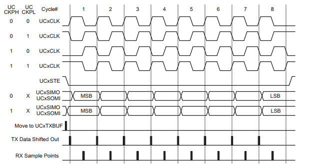
Its important that the right phase and polarity are selected so that the slave and master both capture the bit at the correct clock transition. If this configuration is not correct, you will see garbage coming out, and the slave will not properly receive the data sent by the MSP430. For example, we can see the SPI interface specifications for the CC1101 transceiver:
The CC1101 needs to sample with a rising edge clock at the center of the bit time. Clock Phase = 1 and Phase = 0 are the correct MSP430 master settings in this case.
Although SPI is full-duplex, oftentimes the data sent by the slave is ignored when the master is writing and vice-versa.
The MSP430 family has various peripherals that support SPI. For the MSP430G2553 that is used with the MSP430 Launchpad this includes the USCI peripherals. Other MSP430 devices in other families include the Universal Serial Interface (USI) and the USART Peripheral Interface which also support SPI.
Let’s look at an example of configuring the USCI in the MSP430G2553 for SPI:
// Won't run on MSP430G2553
#include <msp430.h>
int main(void)
{
WDTCTL = WDTPW + WDTHOLD; // Stop WDT
P1OUT |= BIT5;
P1DIR |= BIT5;
P1SEL = BIT1 | BIT2 | BIT4;
P1SEL2 = BIT1 | BIT2 | BIT4;
UCA0CTL1 = UCSWRST;
UCA0CTL0 |= UCCKPH + UCMSB + UCMST + UCSYNC; // 3-pin, 8-bit SPI master
UCA0CTL1 |= UCSSEL_2; // SMCLK
UCA0BR0 |= 0x02; // /2
UCA0BR1 = 0; //
UCA0MCTL = 0; // No modulation
UCA0CTL1 &= ~UCSWRST; // **Initialize USCI state machine**
}
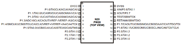
The MSP430G2553 has two SPI interfaces, mapped with the following pins:
UCA0
UCB0
The code above also uses P1.5 as CSn. Why haven’t we used STE? Because STE is not slave select. The Slave Select operation on the MSP430 must be performed using GPIOs. The STE pin, on the other hand, is used when the MSP430 operates as a slave and allows master arbitration. It will not act as a slave select. To enable SPI we need to make the pins for MISO, MOSI and CLK in peripheral mode so USCI will control them. We then configure a custom pin such as P1.5 above, to be the SS or CSn. Looking at the port schematics in the G2553 datasheet we can see that to make the pins work with USCI we need to set Both P1SEL and P1SEL2 to ‘1’.
You might have noticed that we change P1OUT before PDIR, which might seem a bit unnecessary. After all, the output doesn’t take effect unless the direction is Output. The reason for this is that if we were to first set the direction, the output register might have been set to ‘0’. In the time between the output register being 0 and being set to 1, we will cause an undesirable and momentary glitch on the line. The line might go From High Impedance (since by default the pins are in high impedance), to ‘0’ and then to ‘1’. The change from ‘0’ to ‘1’ is mostly harmless, but can sometimes cause issues with devices.
Note that for the cases when we want to use both SPI interfaces, we would need to change CSn from P1.5 to another pin so that P1.5 can be used for UCB0CLK.
With the pinout configured, it’s time to configure the USCI module for operation. As when we configured USCI for UART, we first place the module in reset. We then configure several bits of the UCA0CTL0 register. The code sets the SPI controller to be a Master sending MSB first, which is set by UCMSB and UCMST. UCSYNC selects SPI mode for the module since it supports various protocols and we want to select SPI specifically. UCCKPH enables the right SPI mode for the CC110x transceivers and we use it only as an example. You will need to adjust this for your own device.
As with UART, SPI mode also needs an input clock. The code above selects SMCLK as the source clock for the module with the UCSSEL_2 bit. Just after selecting the clock source, the clock divider is set to device the input clock (SMCLK in this case) by 2. Note that the USCI module must have an input clock divided by at least 2. So, if SMCLK is running at 16MHz, our SPI will run at 8MHz. With the clocks and module configured, we can take the module out of reset and it will be ready to run. Because feeds the master clock to the SPI slave, both master and slave are synchronized which means clock accuracy is not critical. Because of this we don’t have to worry about accurate clocks when using SPI. SPI can theoretically operate at any frequency, but the MSP430 and slave limit the maximum frequency that can be used.
Once out of reset, the SPI peripheral is ready. Let’s see how we transmit a byte. Note that this is a blocking implementation. In practice you will want to use interrupts which will enable the MSP430 to do other things while the SPI module is operating.
// Won't run on MSP430G2553
#include <msp430.h>

volatile char received_ch = 0;
int main(void)
{
    WDTCTL = WDTPW + WDTHOLD; // Stop WDT

    P1OUT |= BIT5;
    P1DIR |= BIT5;
    P1SEL = BIT1 | BIT2 | BIT4;
    P1SEL2 = BIT1 | BIT2 | BIT4;

    UCA0CTL1 = UCSWRST
    UCA0CTL0 |= UCCKPH + UCMSB + UCMST + UCSYNC; // 3-pin, 8-bit SPI master
    UCA0CTL1 |= UCSSEL_2; // SMCLK
    UCA0BR0 |= 0x02; // /2
    UCA0BR1 = 0; //
    UCA0MCTL = 0; // No modulation
    UCA0CTL1 &= ~UCSWRST; // **Initialize USCI state machine**

    P1OUT &= (~BIT5); // Select Device

    while (!(IFG2 & UCA0TXIFG)); // USCI_A0 TX buffer ready?
    UCA0TXBUF = 0xAA; // Send 0xAA over SPI to Slave
    while (!(IFG2 & UCA0RXIFG)); // USCI_A0 RX Received?
    received_ch = UCA0RXBUF; // Store received data

    P1OUT |= (BIT5); // Unselect Device
}
The first thing to do is to select the SPI slave by putting P1.5 low using the P1OUT register. After this we need to check whether the TXIFG flag is set. As with UART, this flag is set when the TX buffer is ready to be filled with data. In our case we know that no other operation has been performed on the SPI module, so there is no reason to check and this is a formality. But it is important to build code that works well in all cases. Note that the while loop waits while the flag is 0 and will exit immediately once the flag is set. As soon as it is, we can send a byte by filling the TXBUF. As soon as TXBUF is filled, the SPI will generate SCLK and transfer the bits. But, how do we know when the transmission is done? We should never interrupt a slave by raising the slave select during a transmission since most devices will interpret that as an aborted transmission and will discard the bits. If you remember, SPI is a duplex protocol which means that the slave also sends back data. In most cases this data is 0x00 or 0xFF (garbage), but we can use the RXIFG flag to wait until the transmission and the reception on the master side is over. After we receive the data, we store the byte received in a variable and then terminate communications by raising P1.5 High again.
With these elements it is possible to build a complete application to talk to one or multiple slaves.
Enter your email address to subscribe to this blog and receive notifications of new posts by email.