One of the first decisions you’ll have to make when you start designing a Bluetooth product is whether you’ll use a module or a discrete Bluetooth chip. We won’t get into the details of which chip to choose since we have a great guide for selecting a Bluetooth chipset. So, we’ll assume that you’ve already chosen your device, and that you also chose to do a discrete design. If your product will be sold in volume, then a discrete design can save on cost.
One of the next decisions is whether to use a QFN or a WLCSP package. Sounds silly right? After all, does it matter which package you use? Yes, it does, and we’ll show you why. We’ll go over some of the key factors in deciding
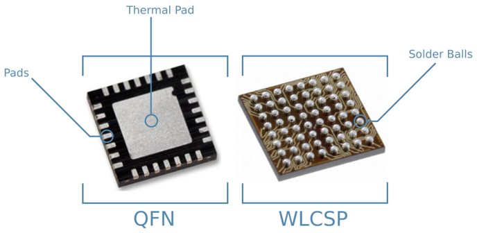
Lowering your costs is critical for almost any BLE product, and it usually starts with selecting the right device. How a device is manufactured has a big effect on the final price. After the manufacturer cuts the silicon die of the device, they have to package it. QFN packaging is complex and involves more raw materials than WLCSP, so it’s more expensive.
In Wafer Level Chip Scale Package (WLCSP) devices, the manufacturer does the bare minimum. Balls and wires are added to the die which is used as the base, without adding a package. A top passivization layer is also added to the device to avoid changing the IC. Less work and materials means that WLCSP is cheaper than QFN.
The differences between the two packages can range between 20 to 40 cents which in volume can translate

The Chip Scale in WLCSP tells you something important, that the whole device is chip scale. If you opened up a BLE part in QFN you’d realize that there is wasted space just because the QFN part has to be big enough to fit all the pads physically.
WLCSP has balls underneath that can occupy the complete area, not just the perimeter, which is much more efficient. So, the device can be physically smaller and have the same or more pads than QFN.
QFN devices for BLE are usually 4mmx4mm, 5mm x 5mm and above while WLCSP can be 3mm x 3mm.
Designing with a QFN is pretty straightforward since all you need to do is break out the device and route the signals. Below is a QFN device with the center Thermal Pad grounding with plenty of vias. The vias help reduce that inductance and improves thermal coupling. Reducing inductance is critical to ensuring good RF performance.
The large area of the QFN Thermal also helps ensure good mechanical attachment which increases reliability.
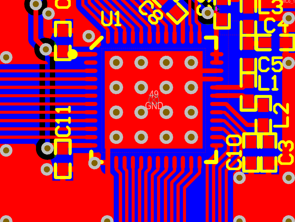
You can see here an image of a routed nRF51822 in QFN package. The routing doesn’t require a lot of vias, but the traces prevent components from being placed close to the device. Not an issue if space is available.
WLCSP on the other hand can be more difficult because of the small pitch of the pads. A pitch of 0.4mm or 0.5mm can make it impossible to route the signals on the inside of the perimeter. Routing these signals will require smaller geometries and vias. The vias in turn require multiple layers to break out. With small BGAs, 4 layers are commonly needed which drives up the cost.
You can sacrifice some of the balls and signals in the center of the, and break out only the outer balls. This way, you only need 2 layers. This saves some of the cost of the PCB but you may not be able to afford losing the signals.
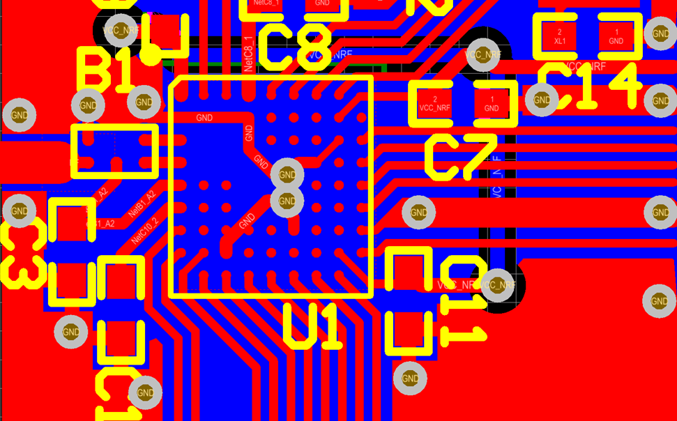
The image above shows a nRF51822 WLCSP device with only the outer balls routed, as well as the ground balls. Nordic Semiconductor has designed the WLCSP to be routable in 2 layers, with standard size vias in an empty space under a package. The disadvantage here is that you are missing many of the connection. You can see plenty of pads on the top layer that are not routed.
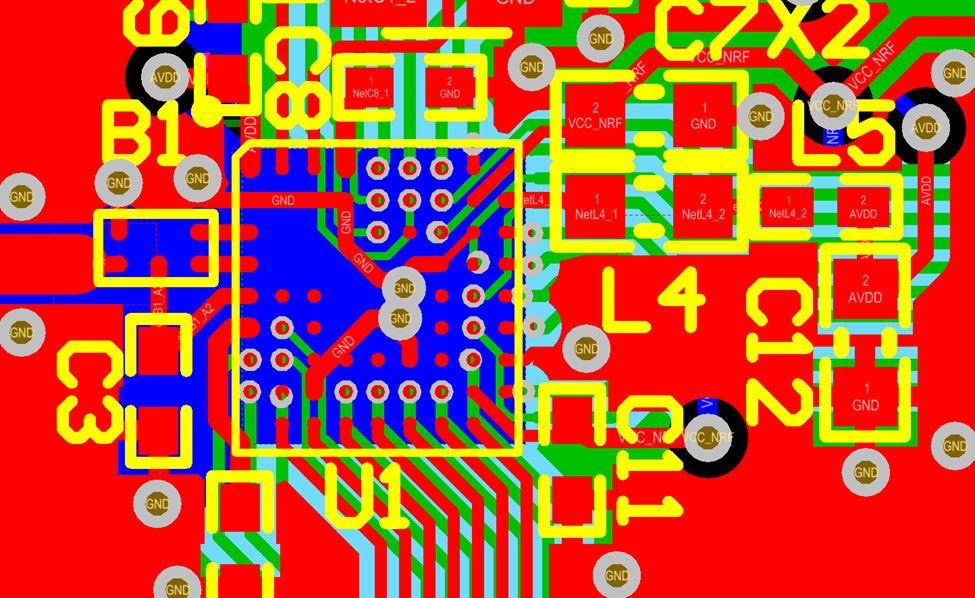
A fully routed nRF51822 device is shown above. Red is the Top layer, while Green is the internal layer. This is a 4 layer design as required to break out the rest of the pins. Some pins are unconnected.
Manufacturing with a QFN part is usually straightforward, and practically all PCB assembly vendors will be able to deal with them. The thermal pad helps with reliability and issues are usually non-existent as long as manufacturer recommendations are followed. They’re also easily hand soldered for replacement.
WLCSP uses balls under the device and fine traces which requires more expertise and more expensive machinery. The tight spacing of the balls and their properties makes it more difficult to get a high yield because the tolerances on the processes (PCB Manufacturing, etching, etc.) need to be much tighter. A lot of care needs to go into mounting BGA parts. For example, a board could develop cracks in the balls if the solder does not cool properly and the PCB isn’t designed well. If something is wrong, X-Raying the board is the only way to see underneath the part.
Because of these issues, it’s important to make sure your manufacturer is familiar with BGA parts and can work with them and the tolerances specified. Contact them early in the design stage so that you know what they can and can’t do.
You can see from all the points we’ve talked about that choosing QFN vs WLCSP isn’t as straightforward as it first seems. Take into account the total cost including manufacturing costs, design time, yield issues, etc.
| QFN | WLCSP/BGA | |
|---|---|---|
| Cost | More expensive due to extra packaging and materials. | Device usually lower cost |
| Design | Simpler to design | PCB may be more expensive due to complexity in design, smaller trace geometry or via sizes |
| Size | Takes up more space | Smallest Size |
| Manufacturing | Usually straightforward, hand assembly possible | Requires specific assembly and experience to ensure high yields |
Enter your email address to subscribe to this blog and receive notifications of new posts by email.